Electronic Components
Metallographic Preparation Solutions by Material
Use this guide for advice on where to start when performing metallographic preparation and analysis on electronic components. Included are tips for achieving the best results for your metallographic application.
Things to consider when working with Electronic Components

Many electronic components contain materials of varying properties. To achieve better results during preparation focus may be put on specific materials. Careful attention to preparation processes can result in excellent quality surface finish.
Depending on the material, there are slight changes that can be made throughout preparation to improve the surface finish of target features. For example, Silicon, copper and FRP may require slightly different process adjustments for optimal results.
Electronic Components Cutting Tips
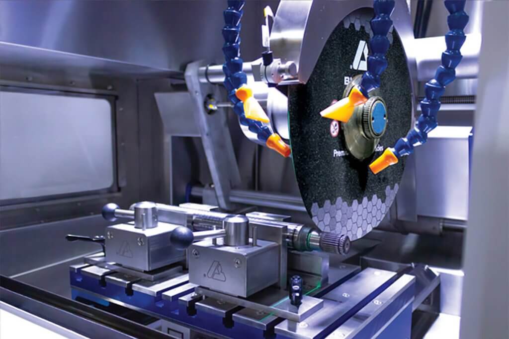
All sectioning should be performed wet, with an ample flow of coolant directed into the cut. Wet cutting will produce a smoother surface finish than a dry cut. Using coolant will also guard against surface damage caused by overheating and mechanical strains. Reducing damage while sectioning is important. Mechanical damage, such as fractures can penetrate deep into the structure and make later preparation steps longer. There are two main types of cutting tools offered: Abrasive and Precision.
Aggressive sectioning can cause mechanical and thermal damage and should be avoided. Due to this, abrasive sectioning is generally not recommended. Precision sectioning results in excellent cut surface quality and can be used to section close to the target area. Cleaving is another option for sectioning silicon wafers.
Precision Cutting Tips
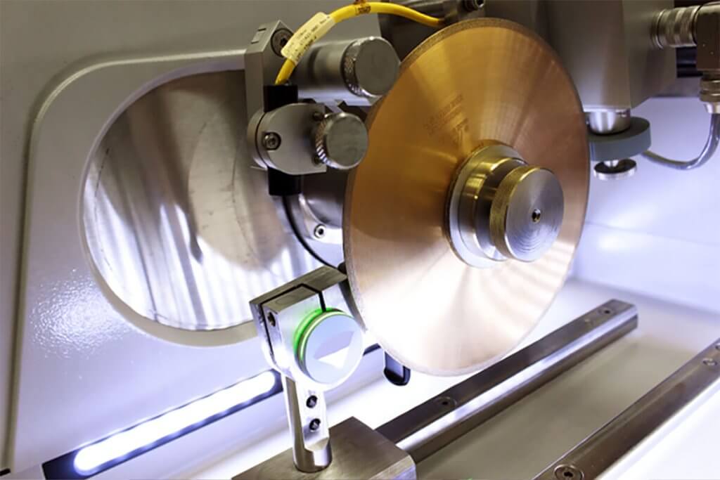
Precision cutters are used in metallographic preparation of electronic components when cutting samples that are small or delicate. Precision blades don’t break down as they are being used. On the outer edge of the blade there is a section where abrasive has been bonded with metal alloy and if taken care of one wafering blade can outlast a box of abrasive blades. Wafering blades can be used with copper for more difficult cuts including making a precise cut close to a feature of interest, or when it is critical to reduce the width of a cut (kerf loss).
Additional benefits of using a precision cutter are a lower load is applied and consequently, less heat is generated, reducing the amount of damage.
Abrasive blades are also made for precision cutters. They can be used in cases where the potential for breaking a blade is high, such as when a part is difficult to clamp, likely to shift during sectioning or there is high variability in the process (ex: multiple operators).
| Recommended Precision blades for Electronic Components | ||||
|---|---|---|---|---|
| Material | 5in (127mm) | 7in (178mm) | 8in (203mm) | Dressing Stick |
| Silicon | 11-4255 0.015in [0.4mm] | 11-4277 0.024in [0.6mm] | 11-479 0.045in [1.1 mm] |
11-1190
11-2490 |
| Other electronic components | 11-4255 0.015in [0.4mm] | 11-4247 0.024in [0.6mm] | 11-4248 0.035in [0.9mm] |
11-1190
11-2490 |
Electronic Components Mounting Tips
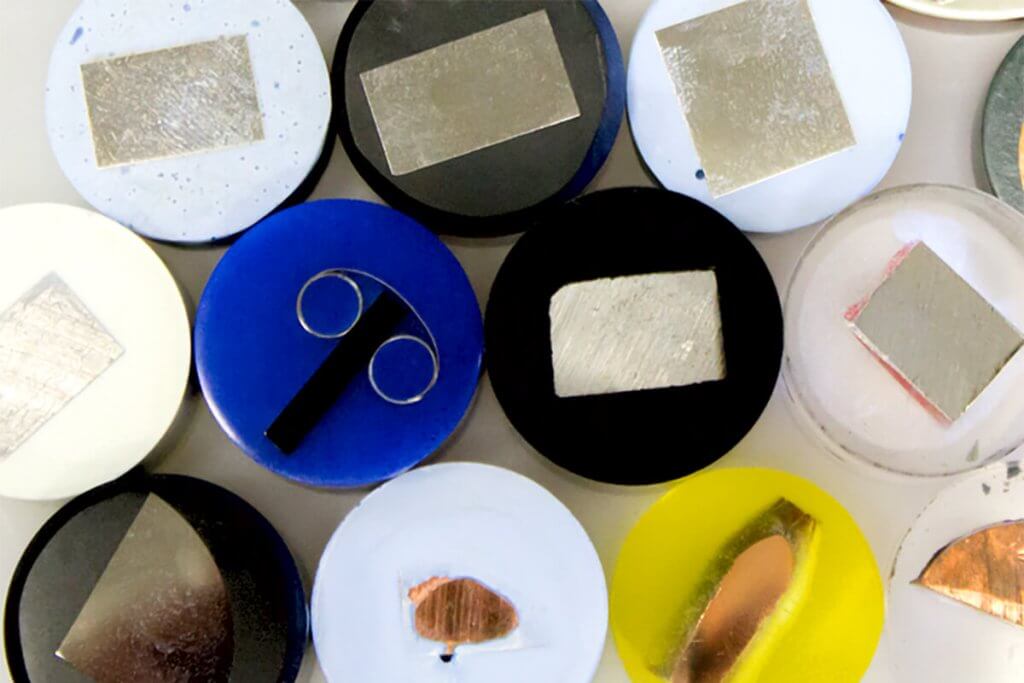
Mounting metallographic samples can allow automation and increase ease of handling during the subsequent steps of metallographic preparation and examination. Intricately shaped samples can be mounted to create uniform shapes allowing automation of the sample preparation process.
Mounting samples also protects and preserves edges or surface defects during metallographic preparation. The method of mounting should in no way alter the microstructure of the specimen. Pressure and heat are the most common sources of injurious effects. Temperatures around 350oF and pressures around 4000 PSI are common for hot compression mounting.
Sample geometry and properties can determine the appropriate method for mounting electronic components. A good quality low viscosity epoxy system such as EpoxiCure® or Epo-Thin® is recommended.
Careful selection can ensure media meets mounting needs regarding timing, viscosity, temperature, and shrinkage. Acrylic systems can increase throughput with quick curing times between 5 and 30 minutes. However acrylic systems are not recommended due to their lower levels of sample adhesion and infiltration. Epoxy systems are the recommended mounting media for electronic components. With lower viscosities and longer working times mixed epoxy can be used with a vacuum system to help penetration levels in intricate geometries.
These small features and intricate geometries can make infiltration difficult. Incomplete infiltration can lead to pores which can complicate analysis leading to errors in measurement. When working with EpoxiCure or EpoThin heating the resin to 40oC in an oven prior to mixing can lower the viscosity and increase infiltration. Pouring under a 22-24 inHg vacuum and cycling samples under vacuum multiple times in short intervals of time, approximately 60 seconds, can also help infiltration of epoxy systems. This cycling can be automated using the SimpliVac vacuum system.
Electronic Components Grinding & Polishing Tips for All Methods

When electronic components contain nonferrous metal and polymers that are the focus then the final polishing step completed should be a MasterPrep® step. Alumina is also better when looking at non-reactive materials like nickel, and gold.
If silicon is being analyzed any grinding done should start with abrasive size no larger than 600 grit. Due to its hard and brittle nature using abrasive larger than 600 grit can lead to significant impact damage. Colloidal silica suspension, like MasterMet®, is better suited to silicon materials and should be used for the final step of the polishing procedure.
Some other materials that colloidal silica is also better suited for are samples like glass, oxides, aluminum, and copper. If Interface analysis is the goal then, fine diamond for the final polishing steps may provide clarity over the oxides.
When eutectic or near eutectic lead solder is of interest the general method below can be used with one slight change. Instead of diamond suspension, paste should be used to reduce the chances of embedding abrasives.
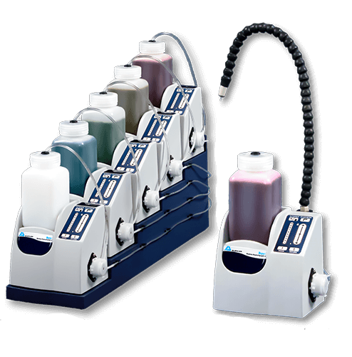
Using Buehler’s Burst dispensing system can conserve diamonds and improve consistency.
The ideal rate for the Burst dispensing system changes with the size of the platen and the polishing cloth that is being used. As a general guideline, for platen size of 8” a burst setting of 3 is a good starting point, for sizes of 10″ and 12″ set the burst system to 4 and adjust as needed. Some experimentation may be required to determine optimal settings to ensure sufficient abrasive and wetting of the cloth. Burst dispensers are also capable of dispensing extenders simultaneously with diamond, if desired.
Loads listed in grinding and polishing methods are recommendations for one 1.25″ mounted specimen. If using central force during preparation the force listed should be multiplied by the number of samples being polished. For different sample sizes, use our load conversion calculator to determine the correct load for your application.
| Method for General Electronic Components | ||||
|---|---|---|---|---|
| Surface | Loads [N] | Base Speed [rpm] | Relative Rotation | Time |
| CarbiMet® 320 grit | 3 [13] | 150 rpm |

|
Hit edge of target |
| TextMet® P with 9um MetaDi® Supreme Diamond | 5 [22] | 150 rpm |

|
5:00 |
| VerduTex with 3um MetaDi Supreme Diamond | 5 [22] | 150 rpm |

|
3:00 |
| VerduTex with 1um MetaDi Supreme Diamond | 5 [22] | 150 rpm |

|
3:00 |
| ChemoMet® with 0.05um MasterPrep® Alumina | 3 [13] | 150 rpm |

|
1:30 |
 = Platen = Platen  = Specimen Holder *Plus MetaDi Fluid Extender as desired = Specimen Holder *Plus MetaDi Fluid Extender as desired
|
||||
| Method for Preparing Silicon in Microelectronics Devices | ||||
|---|---|---|---|---|
| Surface | Loads [N] | Base Speed [rpm] | Relative Rotation | Time |
| CarbiMet® 600 grit | 3 [13] | 100 rpm |

|
Until Plane |
| VerduTex with 6um MetaDi Supreme Diamond | 5 [22] | 100 rpm |

|
3:00 |
| VerduTex with 3um MetaDi Supreme Diamond | 5 [22] | 100 rpm |

|
3:00 |
| VerduTex with 1um MetaDi Supreme Diamond | 5 [22] | 100 rpm |

|
3:00 |
| ChemoMet® with 0.06um MasterMet® Colloidal Silica | 2 [9] | 100 rpm |

|
2:00 |
 = Platen = Platen  = Specimen Holder *Plus MetaDi Fluid Extender as desired = Specimen Holder *Plus MetaDi Fluid Extender as desired
|
||||
Electronic Components Etching Tips
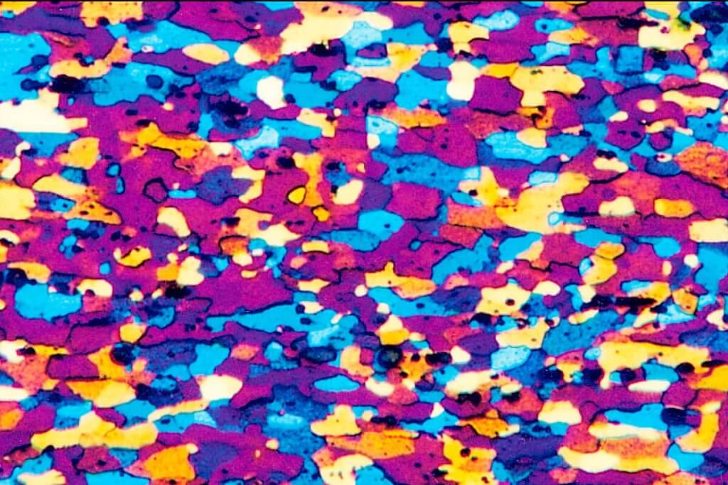
Due to the varying compositions of electronic components, etching practices should be determined by the constituents. Please review the proper pages for etching of different components.
Electronic Components Imaging Tips

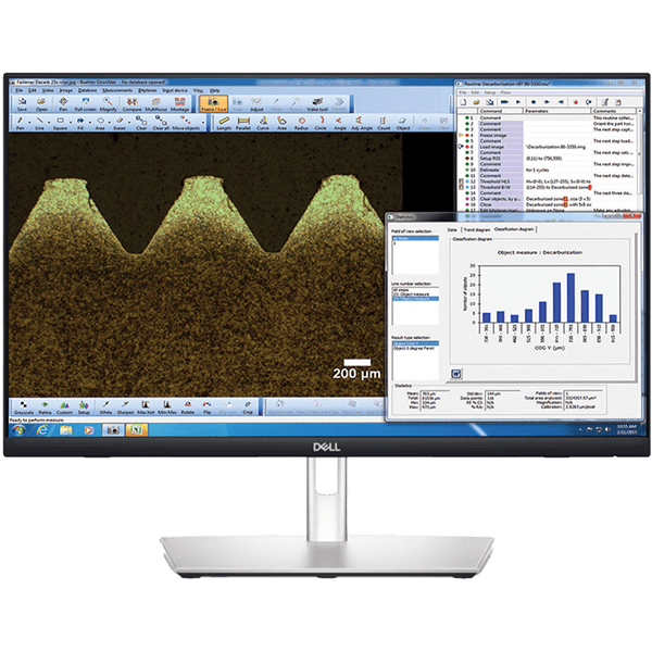
Electronic components can be analyzed to measure a variety of things depending on the composition and application. Some common goals of analysis are feature or defect measurements such as voids, cracks, etchbacks, and contaminants. Dimensional measurements can be taken and saved using our OmniMet® Basic software. For other analysis and exporting needs, more advanced versions of the OmniMet software may be required.
Electronic Components Hardness Testing Tips
| Reference Materials for Hardness Testing | ||
|---|---|---|
| ASTM | ISO | |
| Brinell | E10 | 6506 |
| Rockwell | E18 | 6508 |
| Vickers | E92,E384 | 6507 |
| Knoop | E384 | 4545 |
| Instrumented | E2546 | 14577 |
| Conversions | E140 | 18265 |
| ASM Handbook Volume 8: Mechanical Testing and Evaluation | Hardness Testing Section | |
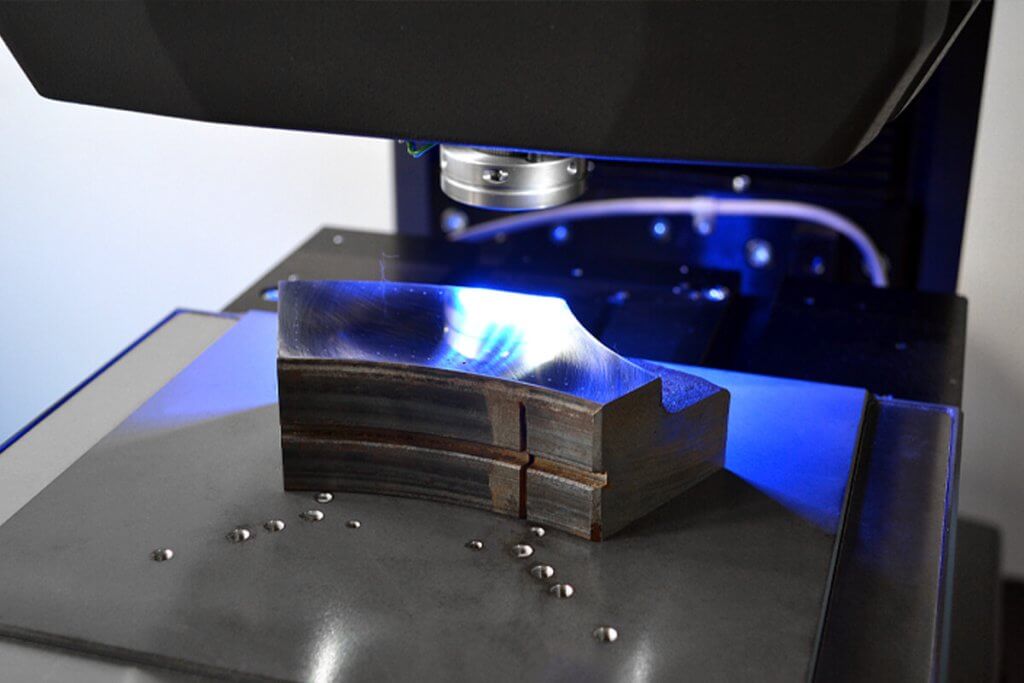
When the method of hardness testing is being determined, the application is assessed to find the scale that meets all needs and standards. At Buehler, our equipment supports hardness testing using four scales: Brinell, Rockwell, Vickers and Knoop. Depending on the information required and the standards to meet, the required scale can change. The table to the side lists several good reference materials for testing methods. In the case of electronic components being smaller in size, Vickers and Knoop testing are common.
The surface finish of the specimen; flatness and scratches could hinder software auto-measuring indents. To reduce uneven surface finish, ensure that the samples are flat before starting the polishing process.
Testing electronic components can be difficult because of differences in reflectance between constituents. Good contrast is important when taking indent measurements. Lighting adjustments may be required for each constituent. Some hardness testing software such as DiaMet Full-automatic have settings to allow automated illumination and focus for each indent made.
Indent tips may be hidden or obscured within pores and cracks. Ceramic constituents are especially susceptible to this. One way to abate these effects when indenting is to use a lighter load. Lighter loads not only decrease the chances of cracking but also allow for the targeting of smaller areas of material. Configure equipment with a 100x objective when measuring indents 20 microns or smaller. Air entrapped within the resin used for mounting could form pores. Pores should be avoided when testing.
Automation and documentation levels are based on the scale used. If automation is needed the different levels of DiaMet available with a tester should be discussed. Adding automation to testing processes can help to increase throughput of analysis systems and repeatability.
Related Products
All Solutions by Material
Choose a material to view Buehler's resources

Find Your Solutions
Full Lab
Metallography Solutions
Do you want to improve your process? Reach out for one-on-one help from our applications experts.

View all Products in the Buehler Product Catalog

Select a method by material
Search Buehler's Safety Data Sheets

Browse and search Buehler's product literature


